-
Product CenterPRODUCT CENTER
-
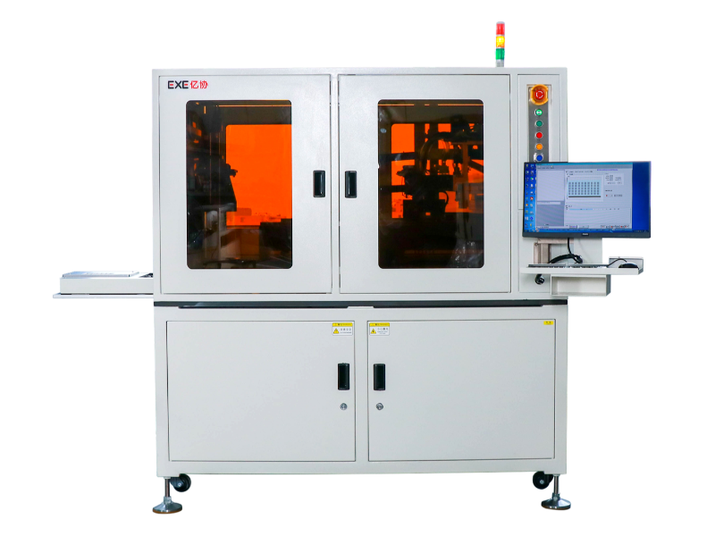
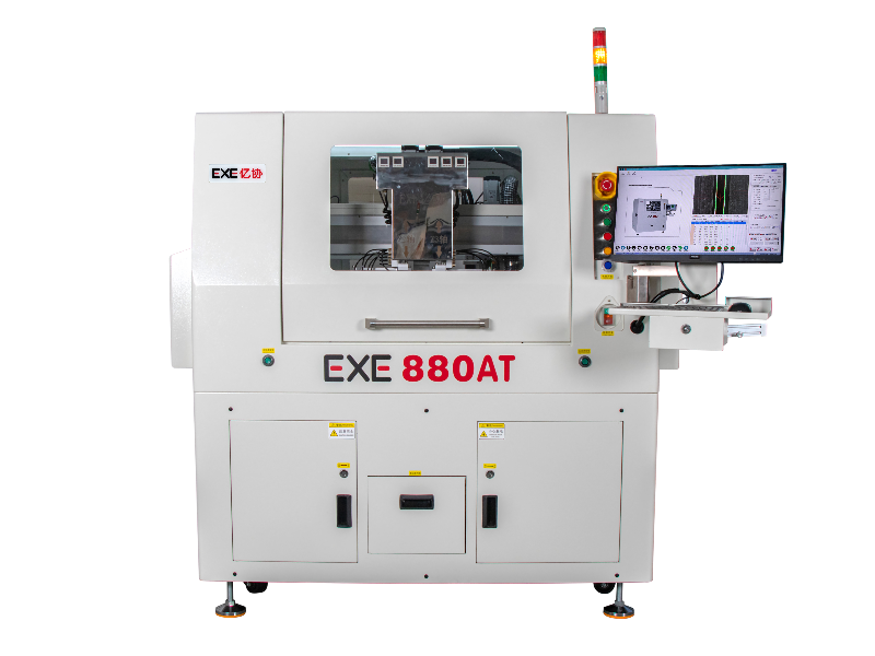
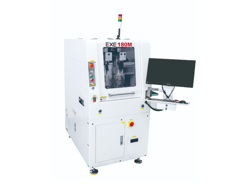
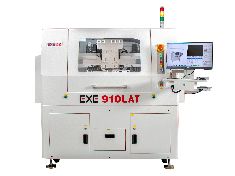
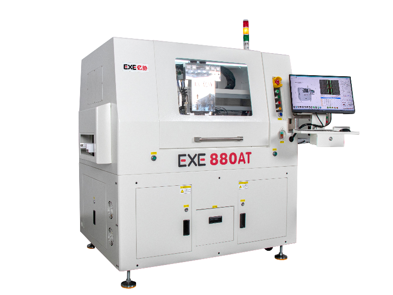
Automatic PCB splitter EXE-880F Dual spindle off-line splitter EXE-910 Vacuum on milling cutter splitter EXE-880F Single platform milling cutter splitter EXE880FS Automatic milling cutter splitter EXE-880 Automatic splitter widener plus large EXE-880XL Vacuum EXE-880 on milling cutter divider Automatic PCB splitter EXE-880L Secondary dust removal machine EXE901
-
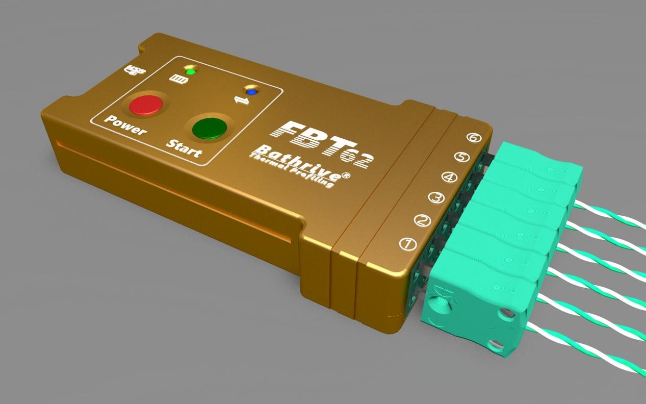
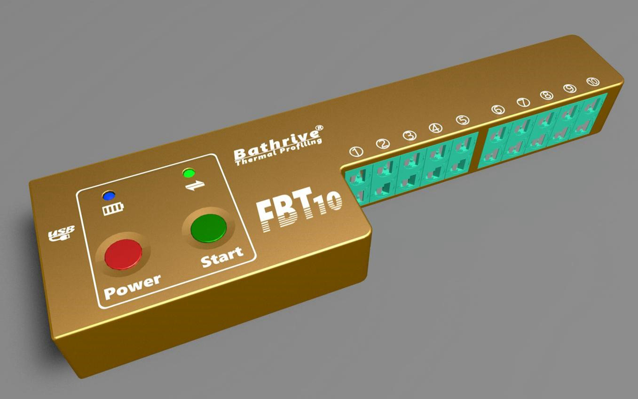
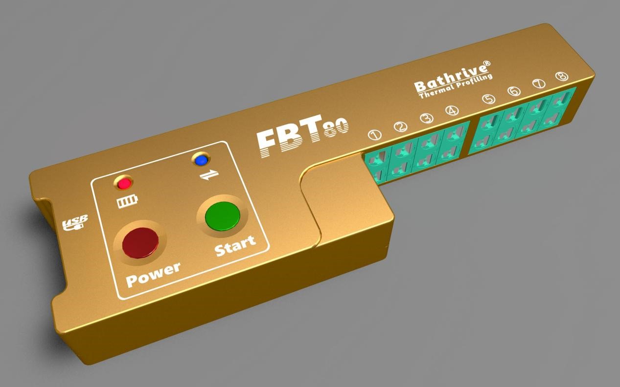
Bride furnace temperature tester FBT24 Bride furnace temperature tester FBT16 Bride furnace temperature tester FBT12 Bride furnace temperature tester FBT10B Bride furnace temperature tester FBT10 Bride furnace temperature tester FBT80 Bride furnace temperature tester FBT62 Bride furnace temperature tester FBT61 Bride furnace temperature tester FBT60 Bride furnace temperature tester FBT42
-
Bride wireless furnace temperature tester GX10 Bride wireless furnace temperature tester GX61 Bride wireless furnace temperature tester GX62 Bride wireless furnace temperature tester GX81 Bride wireless furnace temperature tester GX82 Bride wireless furnace temperature tester GX10B Bride wireless furnace temperature tester GX12 Bride wireless furnace temperature tester GX16 Bride wireless furnace temperature tester GX24

-
Application IndustryIndustry INDUSTRY

-
Company ProfileCOMPANY INTRODUCTION


-
Automatic PCB splitter EXE-880FDual spindle off-line splitter EXE-910Vacuum on milling cutter splitter EXE-880FSingle platform milling cutter splitter EXE880FSAutomatic milling cutter splitter EXE-880Automatic splitter widener plus large EXE-880XLVacuum EXE-880 on milling cutter dividerAutomatic PCB splitter EXE-880LSecondary dust removal machine EXE901
-
Bride furnace temperature tester FBT24Bride furnace temperature tester FBT16Bride furnace temperature tester FBT12Bride furnace temperature tester FBT10BBride furnace temperature tester FBT10Bride furnace temperature tester FBT80Bride furnace temperature tester FBT62Bride furnace temperature tester FBT61Bride furnace temperature tester FBT60Bride furnace temperature tester FBT42Bride furnace temperature tester V6
-
Bride wireless furnace temperature tester GX10Bride wireless furnace temperature tester GX61Bride wireless furnace temperature tester GX62Bride wireless furnace temperature tester GX81Bride wireless furnace temperature tester GX82Bride wireless furnace temperature tester GX10BBride wireless furnace temperature tester GX12Bride wireless furnace temperature tester GX16Bride wireless furnace temperature tester GX24